
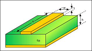
You need to design a microstipy line for a high speed digital signal in a 4 layer PCB. The copper foil thickness of all planes is 35 um. Imagine you have your signal on the bottom layer, which should be the width of the 5.6 GHz signal strap to obtain a 50 Ohms impedance using Wheeler (Gupta, Garg, & Bahl, 1979), Hammerstad (Edwards & Steer, 2016), Ownes (Edwards & Steer, 2016; Kirschning, Jansen, & Koster, 1981), Hammerstad & Jensen (Edwards & Steer, 2016; Kirschning et al., 1981; Wong, 1979), Bahl & Garg [(Wong, 1979) y Kobayashi (Garg & Bahl, 1979).
The solution proposed by a studuent is outlined in this PDF file.